I2C on the STM32 Nucleo-L432KC
Adapted (ctrl-c ctrl-v) from my notes.
Scenario
I have an STM32 NUCLEO-L432KC board and an SSD1306 128x64 OLED screen. I want to display some stuff on the screen. I'll connect the two using the I2C bus and protocol.
I2C bus
The bus connects master to slave via two wires, the Serial Clock Line (SCL) and Serial Data Line (SDA). SCL is used to synchronize messaging. SDA carries the data. The SCL and SDA lines are open drain meaning the chip can only drive 0v on these lines. They must then be connected via pull-ups to VCC. Why does everything seem to work with 4.7k resistors?
Master and Slave
The master drives the clock line and initiates data transfer. There is usually (usually) only one master. Slaves do not initiate data transfers, they only respond. There can be many slaves to a master.
The Protocol
To initiate or terminate a data transfer, the master triggers a start or stop condition. These conditions are unique because they are the only times when the SDA line is allowed to change while the SCL line is high. Specifically, the start condition occurs when the SDA line transitions from high to low while SCL is high, and the stop condition occurs when SDA transitions from low to high while SCL is high. These conditions do not require an acknowledgment. Outside of these conditions, the SDA line must remain stable whenever SCL is high. Data is transmitted one byte at a time on the SDA line, beginning with the most significant bit (MSB). With each SCL pulse, one bit is transferred. After receiving 8 bits, the slave sends an acknowledgment (ACK/NACK) bit. An ACK (low) indicates that the data was received correctly and that the slave is ready for another byte, while a NACK (high) signals that the slave cannot accept more data or that there is no device at the target address, prompting the master to end the transfer with a stop condition.
The address of a device on the I2C bus is 7 bits (or 10 bits but I wont cover that). When sending an address, a full byte plus ACK bit is still sent. The eighth bit is used to specify whether data is to be read or written (R/W). 0 to write, 1 to read. So the full addressing message looks like a 7 bit address (MSB first), R/W bit, and the ACK.
Full write protocol:
1) Send a Start condition.
2) Transmit the target slave address with the write bit; receive an ACK.
3) Transmit the target register address; receive an ACK.
4) Transmit the data packet(s), each followed by an ACK.
5) Send a Stop condition.
Full read protocol:
1) Send a Start condition.
2) Transmit the target slave address with the write bit; receive an ACK.
3) Transmit the target register address; receive an ACK.
4) Send a repeated Start condition.
5) Transmit the target slave address with the read bit; receive an ACK.
6) Receive the data packet(s), sending an ACK after each byte (or a NACK after the final byte).
7) Send a Stop condition.
Notice that during reading the master still controls SCL but the slave is sending data across SDA. If the slave is not ready to send data because it were busy with something else (maybe it's another microprocessor) then problems can occur. This is solved via clock stretching. The slave can hold SCL low until it is ready to send data, such that after receiving the read packet from the master, SCL stays low until the slave is ready to send data, stretching the clock pulse.
Speed
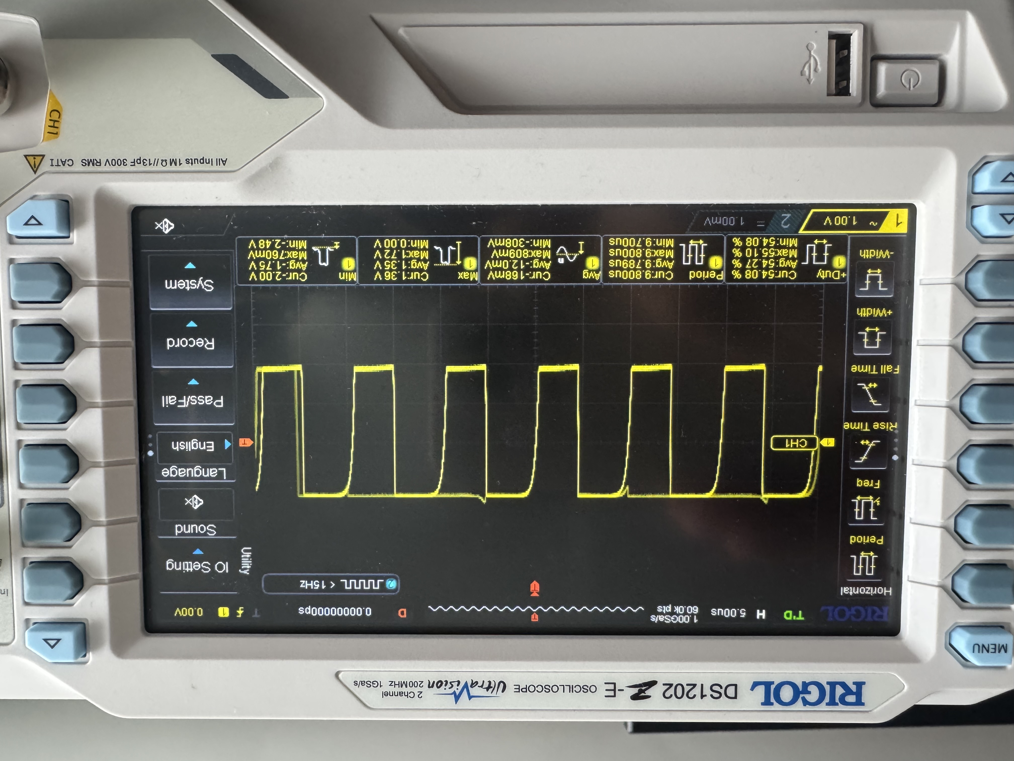
The standard mode SCL speed is 100kHz. Fast mode and High speed mode are 400kHz and 3.4MHz each.
Initializing I2C on the STM32 NUCLEO
To initialize I2C on the STM32 NUCLEO-L432KC, you configure some registers to set up the clock, the I/O pins, as well as the I2C peripheral itself. I'll use pins PB6 and PB7 for I2C1_SCL and I2C1_SDA, respectively. The NUCLEO board supports up to 2 I2C buses (I2C1 and I2C3).
The general procedure is as follows:
1) Clock Configuration - Enable the clock for the I2C peripheral and the associated GPIO ports by setting the Reset and Clock Control (RCC) registers.
2) GPIO Configuration - Set PB6 and PB7 to alternate function mode, selecting the proper alternate function mapping for I2C.
3) I2C Peripheral Initialization - Configure the I2C timing registers to establish the desired SCL frequency (in my case 100kHz for standard mode). This involves setting the clock control parameters and ensuring proper timing characteristics.
Board Clock Configuration
To configure the board clocks I'll configure three registers:
1) RCC_AHB2ENR is the peripheral clock enable register - set bit 0 to 1 to enable the clock for GPIO port B
2) RCC_APB1ENR1 is the I2C clock enable register - set bit 21 to 1 to enable the clock for I2C1
3) RCC_CCIPR is the source clock register - set bits 13:12 to 10 to select the HSI16 clock (a 16 MHz high-speed internal RC oscillator) which I'll use as the source for I2C1
GPIO Pin Configuration
To configure the GPIO pins for I2C1, I'll modify four registers:
1) GPIOB_MODER is used to set the mode of each pin - for pins 6 and 7, set bit fields 12:13 and 14:15 to 10 to select alternate function mode.
2) GPIOB_OTYPER configures the output type - set bits 6 and 7 to 1 to configure the pins as open-drain for I2C communication.
3) GPIOB_PUPDR sets the pull-up/pull-down resistors - for pins 6 and 7, set bit fields 12:13 and 14:15 to 01 to enable pull-up resistors.
4) GPIOB_AFRL assigns the alternate function mapping for pins 6 and 7 - set bits 24:27 and 28:31 to 0100 to select AF4 for I2C1.
I2C Peripheral Initialization
Configuring the I2C1 peripheral is slightly more involved.
1) I2C_CR1 is the control register for our I2C - Begin by disabling the peripheral to ensure that timing parameters can be modified safely. This is done by clearing the Peripheral Enable (PE) bit in position 0. (In my experience it helps to do a software reset here too).
2) Next, configure the timing characteristics by writing an appropriate value to I2C_TIMINGR. This 32-bit register is divided into several fields: the prescaler (PRESC, bits 31:28), which divides the input clock to create a time base; SCLDEL (bits 27:24) and SDADEL (bits 23:20), which introduce delays to satisfy the I2C data setup and hold requirements; and SCLH (bits 15:8) and SCLL (bits 7:0), which determine the durations of the SCL high and low periods.
- First determine the time base t_I2C = (PRESC + 1) / f_I2Csource (where f_I2Csource is 16MHz).
- Then determine the total SCL period T_SCL = (SCLL + SCLH + 2) * t_I2C for 100kHz operation.
- Finally, choose SCLDEL and SDADEL to meet minimum data setup and hold times: T_SCLDEL = (SCLDEL + 1) * t_I2C and T_SDADEL = (SDADEL + 1) * t_I2C.
I used PRESC = 0, SCLL = 80, SCLH = 63, SCLDEL = 4, SDADEL = 2. Note that bits 19:16 are unused so leave them unchanged.
3) Combine these parameters into a single 32-bit value and write it to I2C_TIMINGR.
4) Enable the analog filter, disable the digital filter, and enable error interrupts.
5) Finally, re-enable I2C1 by setting the PE bit in I2C_CR1.
(EDIT: The STM32L43XXX data sheet gives you tables to read off for different operation modes and source clock frequencies.)
Probably a good idea to check your clock signal is good.
Basic I2C Functions
These functions handle the low-level I2C communication by managing start/stop conditions, data transfers, bus status, and error handling:
- I2C_Start
- I2C_Stop
- I2C_Write
- I2C_Read
- I2C_SendAddress
- I2C_ForceReset
- I2C_ClearFlags
- I2C_WaitBusReady
- I2C_PrepareBus
- I2C_Transaction
SSD1306 OLED I2C Functions
These functions encapsulate the process of controlling the OLED display over I2C. There's some stuff to pay attention to in the different addressing modes (page, horizontal, vertical), but I just use horizontal for everything.
- Command Transmission: SSD1306_SendCommand packages a command byte with a control byte (0x00) indicating command mode, then sends the two-byte packet using an I2C transaction.
- Initialization Sequence: SSD1306_Init sends a series of commands to configure the display. This includes:
-- Turning the display off.
-- Setting parameters such as the MUX ratio, display offset, start line, segment remap, COM scan direction, and COM pin configuration.
-- Adjusting contrast, oscillator frequency, and enabling the charge pump.
-- Finally, turning the display on.
- Display Control: Functions like SSD1306_Enable, SSD1306_SetAddressingMode, SSD1306_SetColumnAddress, and SSD1306_SetPageAddress allow dynamic control over display settings and addressing modes.
- Data Handling and Buffer Management:
-- SSD1306_SendData transmits a buffer of display data by prefixing it with a control byte (0x40), which indicates that subsequent bytes are graphic data.
-- The display buffer is organized into 8 pages (each 128 bytes, where each byte represents 8 vertical pixels).
-- Helper functions such as SSD1306_DrawToBuffer, SSD1306_ClearBuffer, SSD1306_FillBuffer, and SSD1306_FlushBuffer manage pixel-level drawing and update the display in one go.
Standard rotating cube demo:
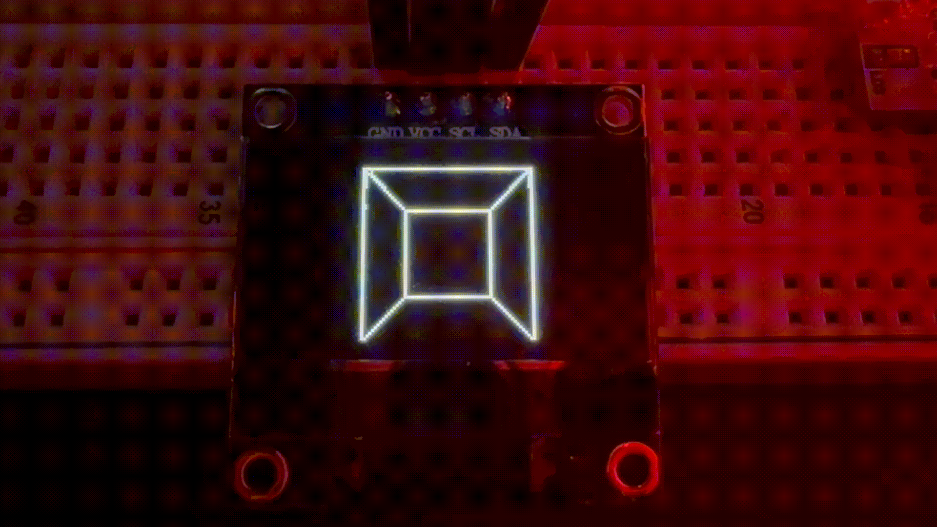
Code at: github